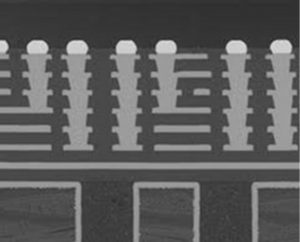
Flip-Chip Package Substrate manufacturers. FC BGA Package Substrate Suppliers. We have made ABF base Package Substrates from 4 layers to 14 layers. Ultra-small line width line spacing from 12um to 35um. and small size BGA pads. and More bigger than 35um line width and line spacing will be easier to produce. we have used the BT materials and ABF materials. there are many types materials. We will produce the high multilayer Flip-Chip Package substrates according to the material you require.
IF you want to know more. See below please. let me explain a little more clearly. Or you can Click on this word to go to our company website: Flip-Chip Package Substrates manufacturers. FC BGA Package Substrate Suppliers.
In this article, we delve into the essential features, advantages, and diverse applications of flip-chip package substrates, highlighting their profound impact on various electronic devices.
Unveiling the Flip-Chip Package Substrate:
The flip-chip package substrate is an advanced packaging technique that directly connects the active side of a semiconductor chip to the substrate using solder bumps. This departure from conventional wire bonding methods eliminates the need for wires and presents several significant advantages. With improved electrical performance, reduced parasitic capacitance and inductance, and efficient heat dissipation, flip-chip package substrates offer unparalleled benefits.
Key Features and Benefits:
- Advancing Miniaturization: Flip-chip package substrates enable remarkable miniaturization of electronic devices by reducing the chip size. Without the constraints of wire bonding, designers can achieve more compact and sleek designs, pushing the boundaries of technological possibilities.
- Enhanced Electrical Performance: The direct chip-to-substrate connection in flip-chip packaging minimizes interconnect lengths and mitigates signal delays. This breakthrough leads to exceptional electrical performance, including higher data transfer rates, reduced power consumption, and improved signal integrity.
- Effective Thermal Management: Compared to wire bonding techniques, flip-chip package substrates offer superior thermal dissipation capabilities. The direct attachment of the chip to the substrate facilitates efficient heat transfer, safeguarding against overheating and enhancing the overall reliability of electronic devices.
- Increased Input/Output Density: Flip-chip package substrates excel in providing a higher input/output (I/O) density, accommodating a larger number of connections between the chip and the substrate. This feature proves invaluable in high-performance applications such as microprocessors, graphic processors, and networking devices.
Wide-ranging Applications of Flip-Chip Package Substrates:
Flip-chip package substrates find widespread applications across various electronic devices, including:
- Microprocessors and Integrated Circuits: Flip-chip package substrates empower microprocessors and integrated circuits in smartphones, tablets, and computers. These substrates unlock faster data processing, improved power efficiency, and reduced form factors, fueling advancements in personal computing.
- High-Speed Communication Devices: High-speed communication devices such as routers, switches, and optical transceivers rely on flip-chip package substrates. With exceptional electrical performance and increased I/O density, these substrates enable lightning-fast data transmission and higher bandwidth, driving the growth of modern networks.
- Advanced Packaging Technologies: Flip-chip package substrates play a pivotal role in advanced packaging technologies like system-in-package (SiP) and three-dimensional integrated circuits (3D-ICs). These technologies demand compact and efficient interconnect solutions, which flip-chip packaging readily provides.
- Automotive Electronics: The automotive industry harnesses the power of flip-chip package substrates in various electronic components, including advanced driver-assistance systems (ADAS), infotainment systems, and engine control units (ECUs). These substrates’ reliability, miniaturization capabilities, and efficient thermal management make them a perfect fit for automotive applications.
Conclusion:
Flip-chip package substrates have emerged as a transformative force in semiconductor packaging, offering unmatched benefits in electrical performance, thermal management, and miniaturization. As the demand for smaller, faster, and more efficient electronic devices continues to soar, flip-chip package substrates will be at the forefront of meeting these evolving needs. Their widespread applications across industries underscore their status as a revolutionary advancement in semiconductor.
When you design the Flip-chip package substrates. If you have any design questions. or If you have any problem with production process capacity or material, please contact our engineers directly. We will help you sincerely and quickly without any consulting fees. Our email: INFO@ALCANTAPCB.COM . Or you can visit our website: ALCANTAPCB.COM